Lattice FPGA iCE40 LP/HX 1280 Cells, 64 kB 160 Blocks, 49-Pin UCBGA
- RS stock no.:
- 772-0085P
- Mfr. Part No.:
- iCE40LP1K-CM49
- Manufacturer:
- Lattice Semiconductor

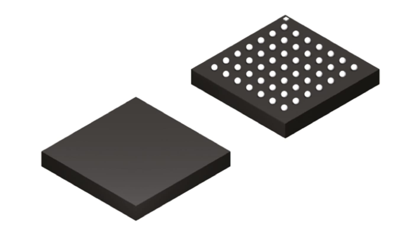
Image representative of range
Stock information currently inaccessible
- RS stock no.:
- 772-0085P
- Mfr. Part No.:
- iCE40LP1K-CM49
- Manufacturer:
- Lattice Semiconductor
Specification
Technical data sheets
Legislation and Compliance
Product Details
Find similar products by selecting one or more attributes.
Select all | Attribute | Value |
|---|---|---|
| Brand | Lattice Semiconductor | |
| Series | iCE40 LP/HX | |
| Product Type | FPGA | |
| Number of Logic Cells | 1280 | |
| Number of Logic Units | 160 | |
| Number of Registers | 1280 | |
| Mount Type | Surface | |
| Package Type | UCBGA | |
| Minimum Supply Voltage | 1.14V | |
| Pin Count | 49 | |
| Maximum Supply Voltage | 1.26V | |
| Minimum Operating Temperature | -40°C | |
| Number of RAM Bits | 64kB | |
| Maximum Operating Temperature | 85°C | |
| Height | 0.9mm | |
| Standards/Approvals | Halogen Free | |
| Length | 3mm | |
| Automotive Standard | No | |
| Select all | ||
|---|---|---|
Brand Lattice Semiconductor | ||
Series iCE40 LP/HX | ||
Product Type FPGA | ||
Number of Logic Cells 1280 | ||
Number of Logic Units 160 | ||
Number of Registers 1280 | ||
Mount Type Surface | ||
Package Type UCBGA | ||
Minimum Supply Voltage 1.14V | ||
Pin Count 49 | ||
Maximum Supply Voltage 1.26V | ||
Minimum Operating Temperature -40°C | ||
Number of RAM Bits 64kB | ||
Maximum Operating Temperature 85°C | ||
Height 0.9mm | ||
Standards/Approvals Halogen Free | ||
Length 3mm | ||
Automotive Standard No | ||
Field Programmable Gate Arrays, Lattice Semiconductor
An FPGA is a semiconductor device consisting of a Matrix of Configurable Logic Blocks (CLBs) connected through programmable interconnects. The user determines these interconnections by programming SRAM. A CLB can be simple (AND, OR gates, etc) or complex (a Block of RAM). The FPGA allows changes to be MADE to a design even after the device is soldered into a PCB.
Related links
- Lattice FPGA iCE40 LP/HX 1280 Cells 49-Pin UCBGA
- Lattice FPGA iCE40LP1K-CM49 iCE40 LP/HX 1280 Cells 49-Pin UCBGA
- Lattice FPGA iCE40 1280 Cells 100-Pin VQFP
- Lattice FPGA iCE40HX1K-VQ100 iCE40 1280 Cells 100-Pin VQFP
- Lattice FPGA iCE40 3520 Cells 144-Pin TQFP
- Lattice FPGA iCE40HX4K-TQ144 iCE40 3520 Cells 144-Pin TQFP
- Lattice Semiconductor Complex Programmable Logic Device ispMACH EEPROM 128 Cells 7.5 ns 36 Labs, In System
- Lattice Semiconductor Complex Programmable Logic Device ispMACH EEPROM 256 Cells 7.5 ns 36 Labs, In System