onsemi MTP3055VL Type N-Channel MOSFET, 12 A, 60 V Enhancement, 3-Pin TO-220
- RS stock no.:
- 761-4542
- Mfr. Part No.:
- MTP3055VL
- Manufacturer:
- onsemi

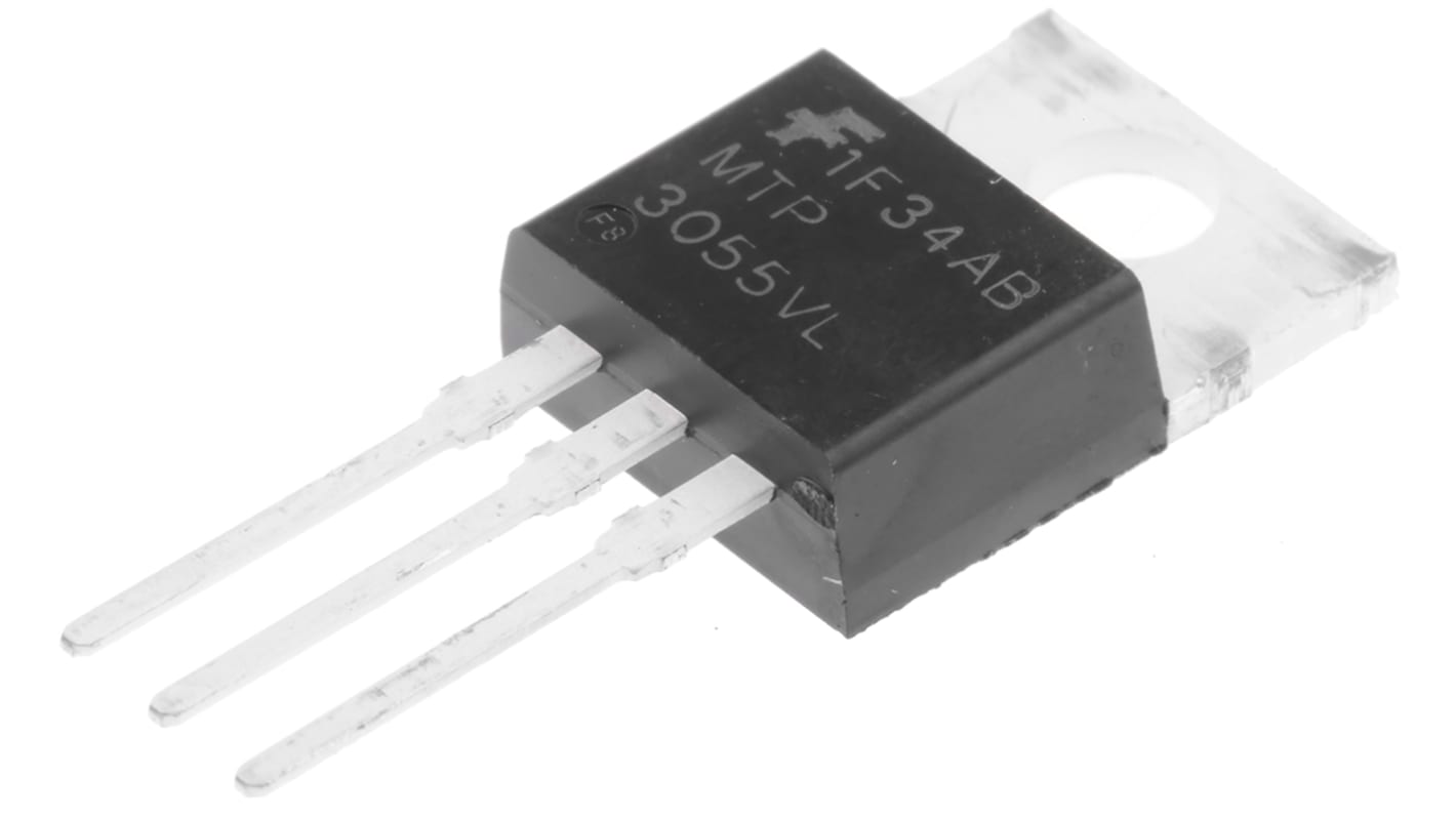
Image representative of range
Bulk discount available
View bulk pricing optionsSubtotal (1 pack of 5 units)*
R 185,77
(exc. VAT)
R 213,635
(inc. VAT)
FREE delivery for orders over R 1,500.00
In Stock
- 65 unit(s) ready to ship from another location
- Plus 800 unit(s) shipping from 02 September 2026
Need more? Click ‘Check delivery dates’ to find extra stock and lead times.
Units | Per unit | Per Pack* |
|---|---|---|
| 5 - 45 | R 37.154 | R 185.77 |
| 50 - 195 | R 36.226 | R 181.13 |
| 200 - 395 | R 35.14 | R 175.70 |
| 400 - 795 | R 33.734 | R 168.67 |
| 800 + | R 32.384 | R 161.92 |
*price indicative
- RS stock no.:
- 761-4542
- Mfr. Part No.:
- MTP3055VL
- Manufacturer:
- onsemi
Specification
Technical data sheets
Legislation and Compliance
Product Details
Find similar products by selecting one or more attributes.
Select all | Attribute | Value |
|---|---|---|
| Brand | onsemi | |
| Channel Type | Type N | |
| Product Type | MOSFET | |
| Maximum Continuous Drain Current Id | 12A | |
| Maximum Drain Source Voltage Vds | 60V | |
| Package Type | TO-220 | |
| Series | MTP3055VL | |
| Mount Type | Through Hole | |
| Pin Count | 3 | |
| Maximum Drain Source Resistance Rds | 180mΩ | |
| Channel Mode | Enhancement | |
| Maximum Power Dissipation Pd | 48W | |
| Typical Gate Charge Qg @ Vgs | 7.8nC | |
| Minimum Operating Temperature | -65°C | |
| Forward Voltage Vf | 1.3V | |
| Maximum Operating Temperature | 175°C | |
| Height | 16.51mm | |
| Length | 10.67mm | |
| Standards/Approvals | No | |
| Automotive Standard | No | |
| Select all | ||
|---|---|---|
Brand onsemi | ||
Channel Type Type N | ||
Product Type MOSFET | ||
Maximum Continuous Drain Current Id 12A | ||
Maximum Drain Source Voltage Vds 60V | ||
Package Type TO-220 | ||
Series MTP3055VL | ||
Mount Type Through Hole | ||
Pin Count 3 | ||
Maximum Drain Source Resistance Rds 180mΩ | ||
Channel Mode Enhancement | ||
Maximum Power Dissipation Pd 48W | ||
Typical Gate Charge Qg @ Vgs 7.8nC | ||
Minimum Operating Temperature -65°C | ||
Forward Voltage Vf 1.3V | ||
Maximum Operating Temperature 175°C | ||
Height 16.51mm | ||
Length 10.67mm | ||
Standards/Approvals No | ||
Automotive Standard No | ||
Enhancement Mode N-Channel MOSFET, Fairchild Semiconductor
Enhancement Mode Field Effect Transistors (FET) are produced using Fairchild’s proprietary, high cell density, DMOS technology. This high density process has been designed to minimise on-state resistance, provide rugged and reliable performance and fast switching.
MOSFET Transistors, ON Semi
ON Semi offers a substantial portfolio of MOSFET devices that includes high-voltage (>250V) and low-voltage (<250V) types. The advanced silicon technology provides smaller die sizes, which it is incorporated into multiple industry-standard and thermally-enhanced packages.
ON Semi MOSFETs provide superior design reliability from reduced voltage spikes and overshoot, to lower junction capacitance and reverse recovery charge, to elimination of additional external components to keep systems up and running longer.
Related links
- onsemi MTP3055VL Type N-Channel MOSFET 60 V Enhancement, 3-Pin TO-220 MTP3055VL
- onsemi NTD3055L104 Type N-Channel MOSFET 60 V Enhancement, 3-Pin TO-252 NTD3055L104T4G
- onsemi NTD3055L104 Type N-Channel MOSFET 60 V Enhancement, 3-Pin TO-252
- onsemi NTD3055-094 Type N-Channel MOSFET 60 V Enhancement, 3-Pin TO-252 NTD3055-094T4G
- onsemi NTD3055-094 Type N-Channel MOSFET 60 V Enhancement, 3-Pin TO-252
- STMicroelectronics STripFET II Type N-Channel MOSFET 60 V Enhancement, 3-Pin TO-252 STD12NF06T4
- STMicroelectronics STripFET II Type N-Channel MOSFET 60 V Enhancement, 3-Pin TO-252 STD12NF06LT4
- STMicroelectronics STripFET II Type N-Channel MOSFET 60 V Enhancement, 3-Pin TO-252