Nexperia Dual Trench MOSFET 2 Type P-Channel Trench MOSFET, 500 mA, -20 V Enhancement, 8-Pin DFN PMDXB950UPELZ
- RS stock no.:
- 152-8344
- Mfr. Part No.:
- PMDXB950UPELZ
- Manufacturer:
- Nexperia

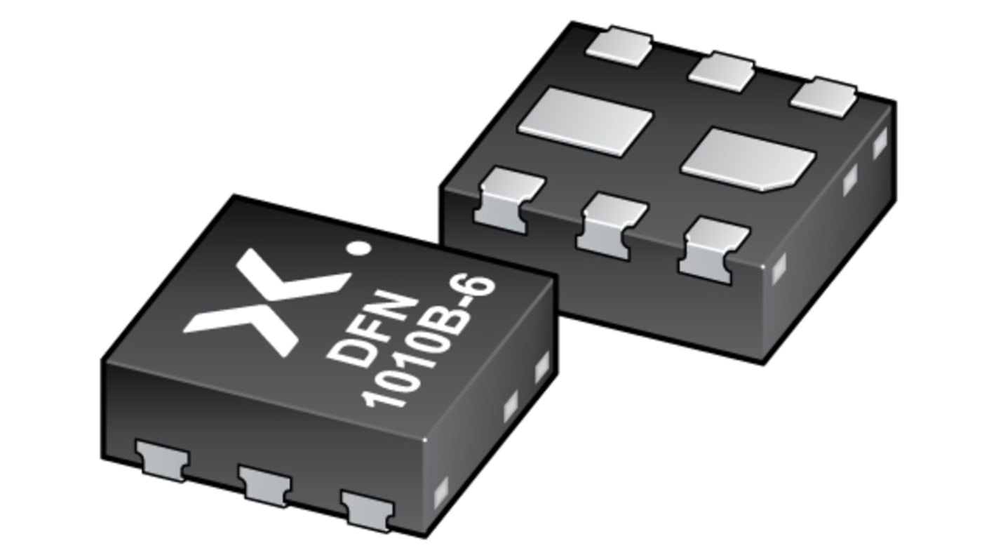
Image representative of range
Bulk discount available
View bulk pricing optionsSubtotal (1 pack of 25 units)*
R 187,625
(exc. VAT)
R 215,775
(inc. VAT)
FREE delivery for orders over R 1,500.00
In Stock
- Plus 7,075 unit(s) shipping from 13 July 2026
Need more? Click ‘Check delivery dates’ to find extra stock and lead times.
Units | Per unit | Per Pack* |
|---|---|---|
| 25 - 100 | R 7.505 | R 187.63 |
| 125 - 1225 | R 7.318 | R 182.95 |
| 1250 - 2475 | R 7.098 | R 177.45 |
| 2500 - 3725 | R 6.814 | R 170.35 |
| 3750 + | R 6.542 | R 163.55 |
*price indicative
- RS stock no.:
- 152-8344
- Mfr. Part No.:
- PMDXB950UPELZ
- Manufacturer:
- Nexperia
Specification
Technical data sheets
Legislation and Compliance
Product Details
Find similar products by selecting one or more attributes.
Select all | Attribute | Value |
|---|---|---|
| Brand | Nexperia | |
| Channel Type | Type P | |
| Product Type | Trench MOSFET | |
| Maximum Continuous Drain Current Id | 500mA | |
| Maximum Drain Source Voltage Vds | -20V | |
| Package Type | DFN | |
| Series | Trench MOSFET | |
| Mount Type | Surface | |
| Pin Count | 8 | |
| Maximum Drain Source Resistance Rds | 3.5Ω | |
| Channel Mode | Enhancement | |
| Maximum Power Dissipation Pd | 4025mW | |
| Minimum Operating Temperature | -55°C | |
| Typical Gate Charge Qg @ Vgs | 1.19nC | |
| Maximum Operating Temperature | 150°C | |
| Transistor Configuration | Dual | |
| Length | 1.15mm | |
| Height | 0.36mm | |
| Standards/Approvals | No | |
| Number of Elements per Chip | 2 | |
| Automotive Standard | No | |
| Select all | ||
|---|---|---|
Brand Nexperia | ||
Channel Type Type P | ||
Product Type Trench MOSFET | ||
Maximum Continuous Drain Current Id 500mA | ||
Maximum Drain Source Voltage Vds -20V | ||
Package Type DFN | ||
Series Trench MOSFET | ||
Mount Type Surface | ||
Pin Count 8 | ||
Maximum Drain Source Resistance Rds 3.5Ω | ||
Channel Mode Enhancement | ||
Maximum Power Dissipation Pd 4025mW | ||
Minimum Operating Temperature -55°C | ||
Typical Gate Charge Qg @ Vgs 1.19nC | ||
Maximum Operating Temperature 150°C | ||
Transistor Configuration Dual | ||
Length 1.15mm | ||
Height 0.36mm | ||
Standards/Approvals No | ||
Number of Elements per Chip 2 | ||
Automotive Standard No | ||
P-channel MOSFETs, The perfect fit for your design when N-channels simply aren’t suitable, Our extensive MOSFET catalog also includes many P-channel device families, based on Nexperia’s leading Trench technology. Rated from 12 V to 70 V and housed in low- and medium-power packages, they offer our familiar blend of high efficiency and high reliability.
20 V, dual P-channel Trench MOSFET, Dual P-channel enhancement mode Field-Effect Transistor (FET) in a leadless ultra small DFN1010B-6 (SOT1216) Surface-Mounted Device (SMD) plastic package using Trench MOSFET technology.
Low leakage current
Trench MOSFET technology
Leadless ultra small and ultra thin SMD plastic package: 1.1 x 1.0 x 0.37 mm
Exposed drain pad for excellent thermal conduction
ElectroStatic Discharge (ESD) protection > 1 kV HBM
Drain-source on-state resistance RDSon = 1.02 Ω
Relay driver
High-speed line driver
High-side load switch
Switching circuits
Related links
- Nexperia Dual Trench MOSFET 2 Type P-Channel Trench MOSFET -20 V Enhancement, 8-Pin DFN
- Nexperia Dual Trench MOSFET 2 Type N-Channel Trench MOSFET 60 V Enhancement, 8-Pin DFN
- Nexperia Dual Trench MOSFET 2 Type N-Channel Trench MOSFET 60 V Enhancement, 8-Pin DFN NX7002BKXBZ
- Nexperia Isolated Trench MOSFET 2 Type P-Channel MOSFET 50 V Enhancement115
- Nexperia Isolated Trench MOSFET 2 Type P-Channel MOSFET 50 V Enhancement, 6-Pin SC-88
- Nexperia Dual NX3008CBKS 2 Type P 350 mA 6-Pin SC-88
- Nexperia Dual NX3008CBKS 2 Type P 350 mA 6-Pin SC-88 NX3008CBKS,115
- Nexperia Dual NX3020NAKS 2 Type N-Channel Trench MOSFET 30 V Enhancement, 6-Pin TSSOP