Toshiba 74HC4050D 6-Channel Buffer & Line Driver, CMOS, Non-Inverting, 16-Pin SOIC
- RS stock no.:
- 171-3601
- Mfr. Part No.:
- 74HC4050D
- Manufacturer:
- Toshiba

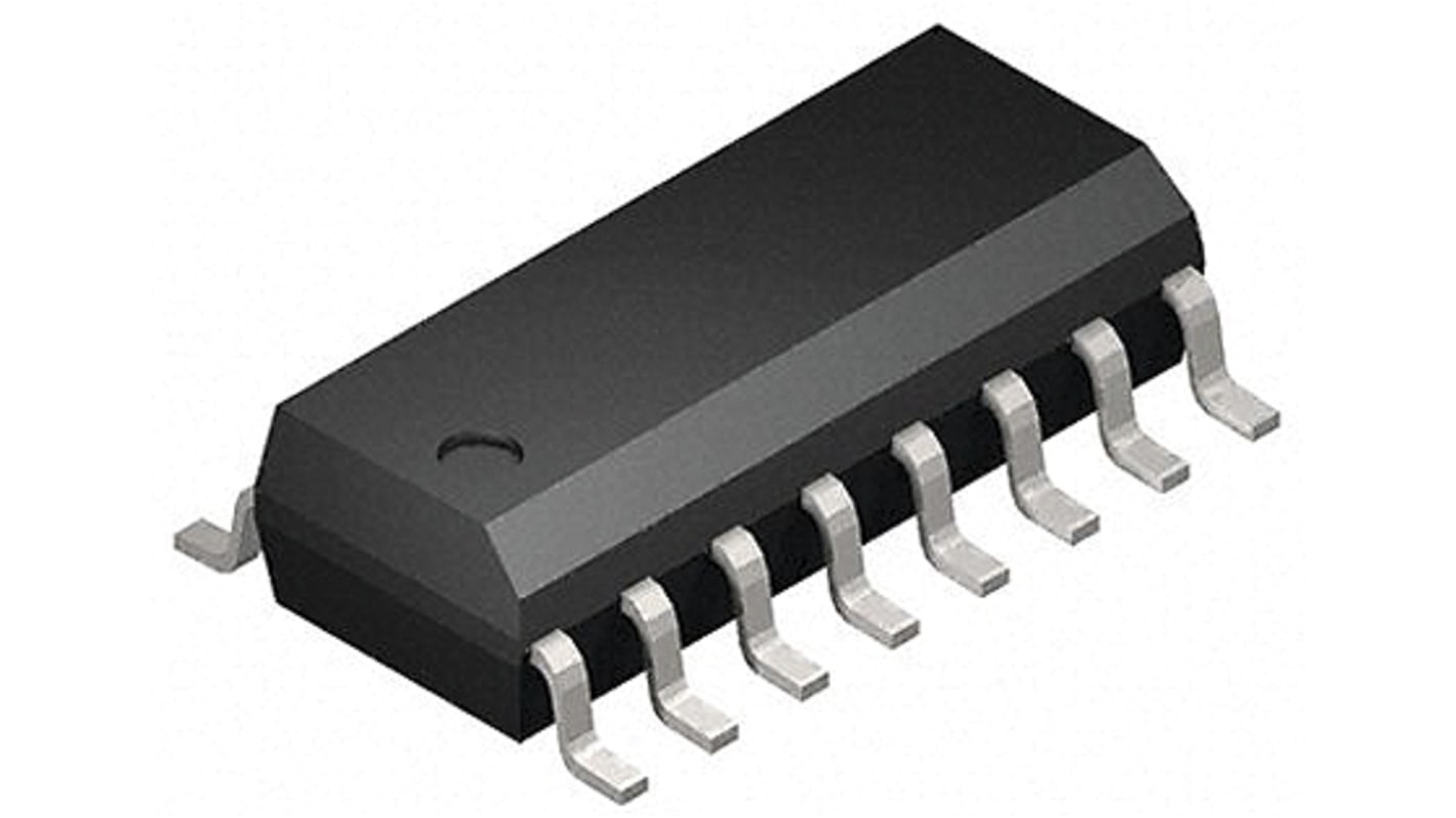
Image representative of range
Bulk discount available
View bulk pricing optionsSubtotal (1 pack of 20 units)*
R 175,12
(exc. VAT)
R 201,38
(inc. VAT)
FREE delivery for orders over R 1,500.00
In Stock
- Plus 180 unit(s) shipping from 27 July 2026
- Plus 740 unit(s) shipping from 03 August 2026
Need more? Click ‘Check delivery dates’ to find extra stock and lead times.
Units | Per unit | Per Pack* |
|---|---|---|
| 20 - 20 | R 8.756 | R 175.12 |
| 40 - 80 | R 8.537 | R 170.74 |
| 100 - 180 | R 8.281 | R 165.62 |
| 200 - 380 | R 7.95 | R 159.00 |
| 400 + | R 7.632 | R 152.64 |
*price indicative
- RS stock no.:
- 171-3601
- Mfr. Part No.:
- 74HC4050D
- Manufacturer:
- Toshiba
Specification
Technical data sheets
Legislation and Compliance
Product Details
Find similar products by selecting one or more attributes.
Select all | Attribute | Value |
|---|---|---|
| Brand | Toshiba | |
| Product Type | Buffer & Line Driver | |
| Logic Family | 74HC | |
| Logic Function | Buffer & Line Driver | |
| IC Type | Hex Buffer | |
| Number of Channels | 6 | |
| Output Type | CMOS | |
| Polarity | Non-Inverting | |
| Mount Type | Surface | |
| Package Type | SOIC | |
| Pin Count | 16 | |
| Minimum Supply Voltage | 2V | |
| Maximum High Level Output Current | -7.8mA | |
| Maximum Supply Voltage | 6V | |
| Minimum Operating Temperature | -40°C | |
| Maximum Propagation Delay Time @ CL | 100ns | |
| Maximum Low Level Output Current | 7.8mA | |
| Maximum Operating Temperature | 85°C | |
| Height | 1.75mm | |
| Length | 10.2mm | |
| Series | 74HC | |
| Standards/Approvals | No | |
| Automotive Standard | No | |
| Supply Current | 10μA | |
| Select all | ||
|---|---|---|
Brand Toshiba | ||
Product Type Buffer & Line Driver | ||
Logic Family 74HC | ||
Logic Function Buffer & Line Driver | ||
IC Type Hex Buffer | ||
Number of Channels 6 | ||
Output Type CMOS | ||
Polarity Non-Inverting | ||
Mount Type Surface | ||
Package Type SOIC | ||
Pin Count 16 | ||
Minimum Supply Voltage 2V | ||
Maximum High Level Output Current -7.8mA | ||
Maximum Supply Voltage 6V | ||
Minimum Operating Temperature -40°C | ||
Maximum Propagation Delay Time @ CL 100ns | ||
Maximum Low Level Output Current 7.8mA | ||
Maximum Operating Temperature 85°C | ||
Height 1.75mm | ||
Length 10.2mm | ||
Series 74HC | ||
Standards/Approvals No | ||
Automotive Standard No | ||
Supply Current 10μA | ||
The 74HC4049D and 74HC4050D are high speed CMOS HEX BUFFERs fabricated with silicon gate C2MOS technology. They achieve the high speed operation similar to equivalent LSTTL while maintaining the CMOS low power dissipation. The 74HC4049D is an inverting buffer, while the 74HC4050D is a non-inverting buffer. The internal circuits are composed of 3-stages (74HC4049D) or 2-stages (74HC4050D) of inverter, which provided high noise immunity and stable output. Input protection circuits are different from those of other high speed CMOS IC's. They eliminate the diodes on the VCC side thus providing of logic-level conversion from high-level voltages up to 15 V to low-level voltages. They are useful for battery back up circuits, because input voltage can be applied on IC's which are not biased by VCC
High speed: tpd = 8 ns (typ.) at VCC = 6.0 V
Low power dissipation: ICC = 1.0 μA (max) at Ta = 25
Balanced propagation delays: tPLH ≈ tPHL
Wide operating voltage range: VCC(opr) = 2.0 V to 6.0 V
Related links
- Toshiba 6-Channel Buffer & Line Driver Non-Inverting, 16-Pin SOIC
- Nexperia 74HC4050D Non-Inverting, 16-Pin SOIC
- Texas Instruments CD74HCT365M 6-Channel Buffer & Line Driver 3 State 16-Pin SOIC
- onsemi MC74HC245ADWG Buffer & Line Driver Non-Inverting, 20-Pin SOIC
- Texas Instruments CD74HC365E 6-Channel Buffer & Line Driver Non-Inverting, 16-Pin PDIP
- onsemi MC74HC245ADTG Buffer & Line Driver Non-Inverting, 20-Pin TSSOP
- Texas Instruments 6-Channel Buffer & Line Driver Non-Inverting, 14-Pin SOIC
- Nexperia 74LVC07AD Open Drain 14-Pin SOIC