Lattice FPGA ICE40HX1K-TQ144, iCE40 HX 1280 Cells, 64kbit, 160 Blocks, 144-Pin TQFP
- RS stock no.:
- 168-4219
- Mfr. Part No.:
- ICE40HX1K-TQ144
- Manufacturer:
- Lattice Semiconductor

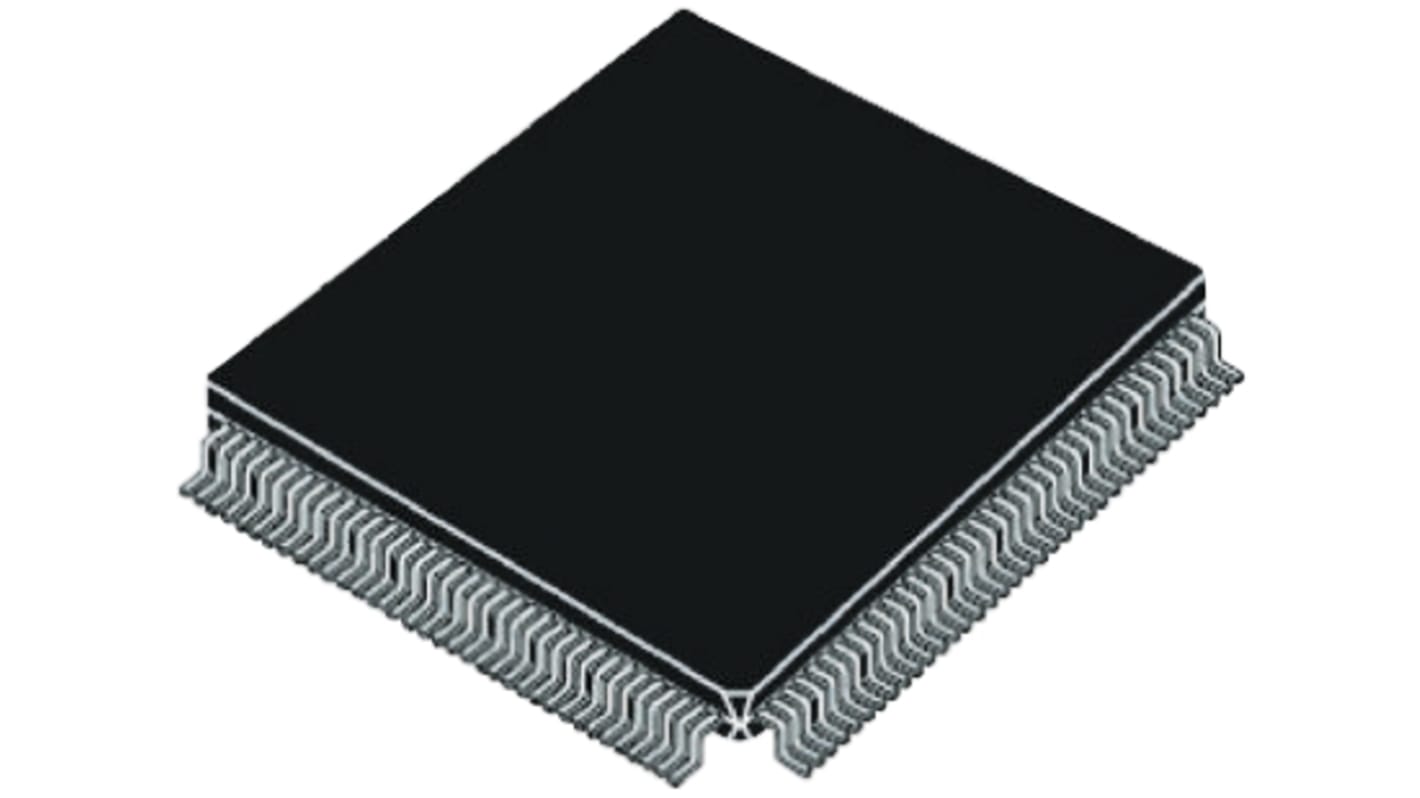
Image representative of range
Unavailable
RS will no longer stock this product.
- RS stock no.:
- 168-4219
- Mfr. Part No.:
- ICE40HX1K-TQ144
- Manufacturer:
- Lattice Semiconductor
Specification
Technical data sheets
Legislation and Compliance
Product Details
Find similar products by selecting one or more attributes.
Select all | Attribute | Value |
|---|---|---|
| Brand | Lattice Semiconductor | |
| Family Name | iCE40 HX | |
| Number of Logic Cells | 1280 | |
| Number of Logic Units | 160 | |
| Number of Registers | 1280 | |
| Mounting Type | Surface Mount | |
| Package Type | TQFP | |
| Pin Count | 144 | |
| Number of RAM Bits | 64kbit | |
| Dimensions | 20 x 20 x 1.45mm | |
| Height | 1.45mm | |
| Length | 20mm | |
| Minimum Operating Supply Voltage | 1.14 V | |
| Maximum Operating Supply Voltage | 1.26 V | |
| Minimum Operating Temperature | -40 °C | |
| Width | 20mm | |
| Maximum Operating Temperature | +85 °C | |
| Select all | ||
|---|---|---|
Brand Lattice Semiconductor | ||
Family Name iCE40 HX | ||
Number of Logic Cells 1280 | ||
Number of Logic Units 160 | ||
Number of Registers 1280 | ||
Mounting Type Surface Mount | ||
Package Type TQFP | ||
Pin Count 144 | ||
Number of RAM Bits 64kbit | ||
Dimensions 20 x 20 x 1.45mm | ||
Height 1.45mm | ||
Length 20mm | ||
Minimum Operating Supply Voltage 1.14 V | ||
Maximum Operating Supply Voltage 1.26 V | ||
Minimum Operating Temperature -40 °C | ||
Width 20mm | ||
Maximum Operating Temperature +85 °C | ||
- COO (Country of Origin):
- KR
Field Programmable Gate Arrays, Lattice Semiconductor
An FPGA is a semiconductor device consisting of a matrix of Configurable Logic Blocks (CLBs) connected through programmable interconnects. The user determines these interconnections by programming SRAM. A CLB can be simple (AND, OR gates, etc) or complex (a block of RAM). The FPGA allows changes to be made to a design even after the device is soldered into a PCB.