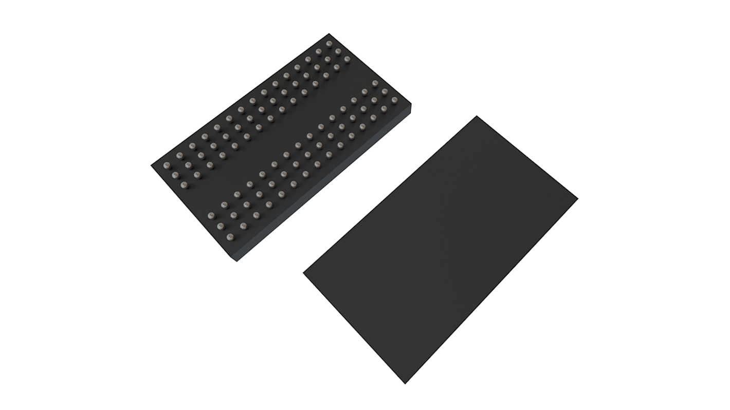
Winbond W9712G6KB25I, SDRAM 128Mbit Surface Mount, 200MHz, 1.7 V to 1.9 V, 84-Pin TFBGA

- RS stock no.:
- 188-2730
- Mfr. Part No.:
- W9712G6KB25I
- Manufacturer:
- Winbond
On back order for despatch 2024/11/28
Not Available for premium delivery
Added
Price (Excl VAT) Each (In a Pack of 5)
R 44,766
(exc. VAT)
R 51,481
(inc. VAT)
| Units | Per unit | Per Pack* |
| 5 - 5 | R 44,766 | R 223,83 |
| 10 - 15 | R 43,646 | R 218,23 |
| 20 - 45 | R 42,336 | R 211,68 |
| 50 - 95 | R 40,642 | R 203,21 |
| 100 + | R 39,016 | R 195,08 |
| *price indicative | ||
- RS stock no.:
- 188-2730
- Mfr. Part No.:
- W9712G6KB25I
- Manufacturer:
- Winbond
Technical data sheets
Legislation and Compliance
Product Details
The W9712G6KB is a 128M bits DDR2 SDRAM and speed involving -25, 25I and -3.
Double Data Rate architecture: two data transfers per clock cycle
CAS Latency: 3, 4, 5 and 6
Burst Length: 4 and 8
Bi-directional, differential data strobes (DQS and /DQS ) are transmitted / received with data
Edge-aligned with Read data and center-aligned with Write data
DLL aligns DQ and DQS transitions with clock
Differential clock inputs (CLK and /CLK)
Data masks (DM) for write data
Commands entered on each positive CLK edge, data and data mask are referenced to both edges of /DQS
Posted /CAS programmable additive latency supported to make command and data bus efficiency
Read Latency = Additive Latency plus CAS Latency (RL = AL + CL)
Off-Chip-Driver impedance adjustment (OCD) and On-Die-Termination (ODT) for better signal quality
Auto-precharge operation for read and write bursts
Auto Refresh and Self Refresh modes
Precharged Power Down and Active Power Down
Write Data Mask
Write Latency = Read Latency - 1 (WL = RL - 1)
Interface: SSTL_18
Specification
Attribute | Value |
|---|---|
| Memory Size | 128Mbit |
| Organisation | 16M x 8 bit |
| SDRAM Class | DDR2 |
| Data Rate | 200MHz |
| Data Bus Width | 16bit |
| Address Bus Width | 15bit |
| Number of Bits per Word | 8bit |
| Maximum Random Access Time | 0.4ns |
| Number of Words | 16M |
| Mounting Type | Surface Mount |
| Package Type | TFBGA |
| Pin Count | 84 |
| Dimensions | 12.6 x 8.1 x 0.8mm |
| Height | 0.8mm |
| Length | 12.6mm |
| Maximum Operating Supply Voltage | 1.9 V |
| Width | 8.1mm |
| Minimum Operating Temperature | -40 °C |
| Minimum Operating Supply Voltage | 1.7 V |
| Maximum Operating Temperature | +95 °C |