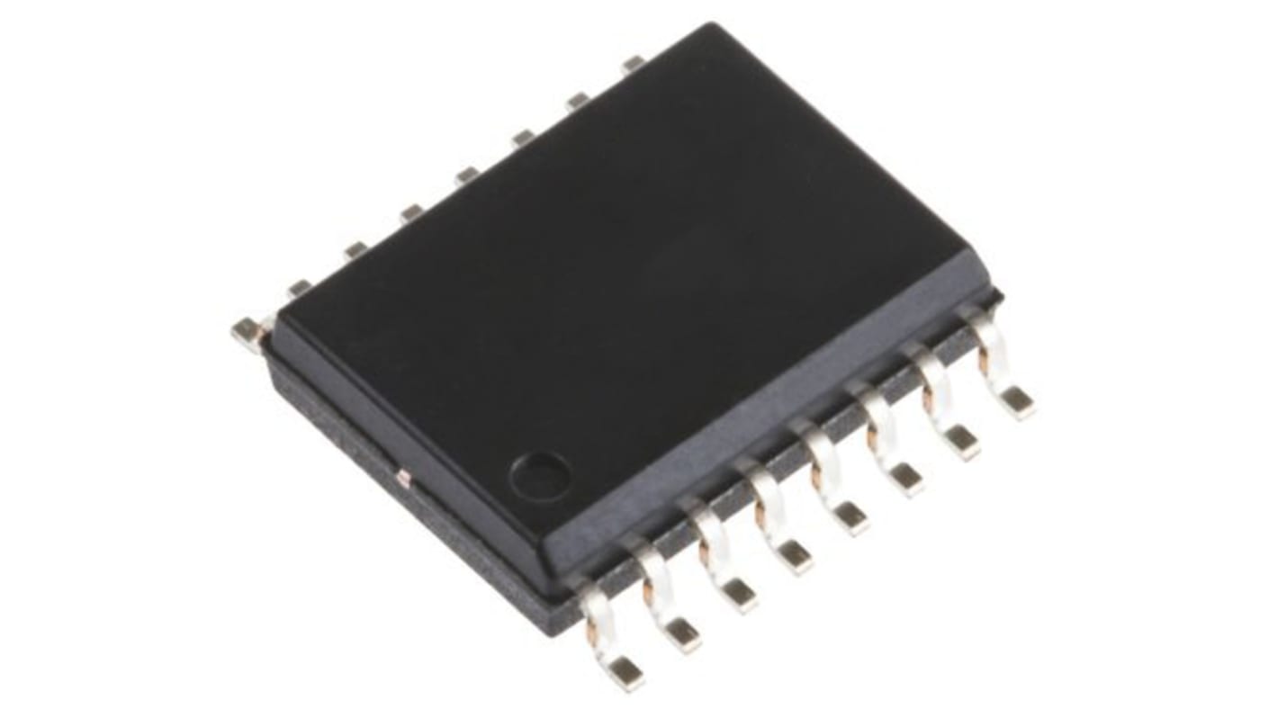
onsemi MC14049UBDG- Hex Hex Inverter, 16-Pin SOIC

- RS stock no.:
- 184-4253
- Mfr. Part No.:
- MC14049UBDG
- Manufacturer:
- onsemi
1872 Available from UK/Europe in 4–6 working days for collection or delivery to major cities (Heavy, hazardous or lithium product excluded. Delivery T&C's apply)
Not Available for premium delivery
Added
Price (Excl VAT) Each (In a Tube of 48)
R 4,833
(exc. VAT)
R 5,558
(inc. VAT)
| Units | Per unit | Per Tube* |
| 48 - 432 | R 4,833 | R 231,984 |
| 480 - 912 | R 4,712 | R 226,176 |
| 960 + | R 4,57 | R 219,36 |
| *price indicative | ||
- RS stock no.:
- 184-4253
- Mfr. Part No.:
- MC14049UBDG
- Manufacturer:
- onsemi
Technical data sheets
Legislation and Compliance
- COO (Country of Origin):
- CN
Product Details
The MC14049UB hex inverter buffer is constructed with MOS P channel and N channel enhancement mode devices in a single monolithic structure.This complementary MOS device finds primaryuse where low power dissipation and or high noise immunity is desired. This device provides logic level conversion using only one supply voltage VDD. The input signal high level VIH can exceed the VDD supply voltage for logic level conversions.Two TTL DTL Loads can be driven when the device is used as CMOS to TTL DTL converters VDD = 5.0 V, VOL 0.4 V IOL 3.2 mA. Note that pins 13 and 16 are not connected internally on this device consequently connections to these terminals will not affect circuit operation.
High Source and Sink Currents
High-to-Low Level Converter
Supply Voltage Range = 3.0 V to 18 V
VIN can exceed VDD
Improved ESD Protection on All Inputs
Pb-Free Packages are Available
High-to-Low Level Converter
Supply Voltage Range = 3.0 V to 18 V
VIN can exceed VDD
Improved ESD Protection on All Inputs
Pb-Free Packages are Available
Specification
Attribute | Value |
|---|---|
| Logic Function | Buffer, Inverter |
| Input Type | CMOS |
| Number of Elements per Chip | 6 |
| Maximum Propagation Delay Time @ Maximum CL | 120ns |
| Maximum High Level Output Current | -4.7mA |
| Maximum Low Level Output Current | 30mA |
| Mounting Type | Surface Mount |
| Package Type | SOIC |
| Pin Count | 16 |
| Dimensions | 10 x 4 x 1.5mm |
| Maximum Operating Supply Voltage | 18 V |
| Height | 1.5mm |
| Width | 4mm |
| Minimum Operating Temperature | -55 °C |
| Maximum Operating Temperature | +125 °C |
| Minimum Operating Supply Voltage | 3 V |
| Propagation Delay Test Condition | 50pF |
| Automotive Standard | AEC-Q100 |
| Length | 10mm |